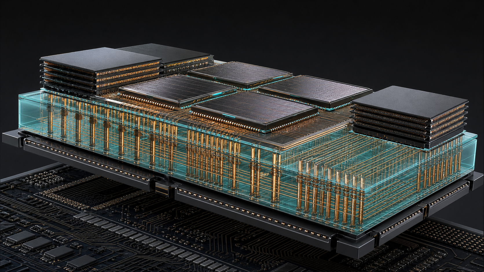
The accelerator package is running out of room long before the rack does. Modern AI processors combine compute tiles, high-bandwidth memory, I/O die and power-delivery structures inside one assembly, and the material beneath those parts has to keep every connection aligned. That substrate rarely appears on a server quotation. It still sets limits that chip designers cannot ignore.
Intel and Lens Technology announced a strategic collaboration on 24 July 2026 to explore glass-substrate packaging and the manufacturing processes needed to scale it. The announcement does not introduce a processor, accelerator or server that buyers can order. It concerns a manufacturing route for future packages, with Intel contributing semiconductor architecture and packaging work while Lens contributes glass processing, laser manufacturing and volume-production experience.
Why should a GPU infrastructure buyer care about something buried inside a package? Because package-level limits eventually appear as system-level compromises: fewer chiplets, longer electrical paths, a smaller memory perimeter, tighter cooling margins or more power spent moving data. Glass will not fix every one of those problems, but it could give package designers more room to work.
This article separates Intel's published claims from the practical consequences. GPUMachines has not tested a glass-core package, and Intel has not named a generally available AI accelerator produced under this new collaboration.
Executive Summary
- What changed: Intel and Lens Technology will explore glass-substrate materials, precision processing and manufacturing methods for future AI and data-centre packages.
- Why glass is under consideration: Intel says glass offers better dimensional, thermal and mechanical stability than current organic substrate materials, supporting denser wiring and larger packages.
- What buyers can purchase today: nothing from this announcement. It is a development and manufacturing agreement, not a product launch.
- Where it may matter first: large AI, HPC and graphics packages that need many chiplets, HBM stacks, high-speed links and dense power delivery.
- What remains unknown: product dates, qualified package designs, yields, cost, service implications and which future processors will use the technology.
Teams planning current infrastructure should continue to select shipping platforms on measured workload fit. GPUMachines can help buyers compare HGX servers, PCIe GPU server architecture and cluster deployment through the GPU Cluster Configurator.
What Intel and Lens Technology Announced
The wording matters. Intel and Lens Technology describe a strategic collaboration focused on possible areas of cooperation in advanced semiconductor packaging. Their stated interests include glass substrate research, precision processing, laser manufacturing and the production techniques required to scale package assembly.
Intel's announcement also names possible later work around structural and thermal components for data-centre servers, AI PCs, robotics and edge systems. Those are areas for exploration. They are not confirmed products, orders or compatibility commitments.
Lens Technology is relevant because glass for semiconductor packaging is not interchangeable with window glass or a display cover. Package substrates need tightly controlled material properties, fine features, repeatable vias, clean surfaces and manufacturing tolerances that survive assembly and thermal cycling. A laboratory coupon can prove a material idea; supplying large, reliable substrates at commercial yield is a different job.
Intel has worked on glass substrates for more than a decade. In 2023, the company said it planned to introduce complete solutions in the latter part of the decade. Its 2026 announcement shows continued ecosystem work, but it does not confirm that the earlier schedule now applies to a named processor.
What a Package Substrate Actually Does
A substrate sits between the semiconductor package and the system board. It provides a mechanical base, carries power and signals, and translates the tiny connection pitch used by chiplets into a larger pitch that a socket or motherboard can accept. Intel engineer Srini Pietambaram has described the substrate as a space transformer, which is a useful plain-English summary.
The job becomes harder as package size and complexity increase. A large AI accelerator may place several compute tiles beside HBM stacks and I/O structures. Each part needs short, predictable paths. Power has to reach rapidly changing loads without excessive voltage loss. Signals must cross the package at high speed without unacceptable interference. The assembled package then heats and cools thousands of times during its service life.
Organic substrates have served the industry well. They can carry dense copper routing and they support existing high-volume processes. The problem is not that organic material suddenly stops working. The problem is how its dimensional behaviour, flatness and feature limits scale when the package grows and the wiring pitch shrinks.
At some point, a designer must either accept longer routes, divide the package differently, add intermediate silicon, reduce its size or move to another substrate material. Glass is one candidate for that next step.
Why AI Packages Put Pressure on Organic Substrates
AI accelerator performance depends heavily on data movement. Compute units need a steady stream of operands from local memory, neighbouring tiles and other accelerators. More HBM bandwidth and more die-to-die links demand more package connections, yet a package cannot grow without consequences.
Large organic substrates can warp during manufacturing and temperature changes. Even a small change across a wide package makes fine-layer alignment harder. Layer-to-layer overlay errors restrict how narrow traces and spaces can become, while uneven surfaces complicate lithography and component attachment.
Power delivery adds another constraint. High-current devices need a dense network of conductors, capacitors and other structures close to the silicon. Signal routing competes for some of the same physical area. A package designer may know how to add another compute tile but lack a clean way to connect and feed it.
HBM placement is equally unforgiving. Moving a memory stack farther from compute affects path length and package geometry. Adding more stacks expands the perimeter or forces a different arrangement. Glass does not create memory bandwidth by itself; it may allow denser, more stable routing around the parts that provide it.
These are package design issues, not evidence that any current GPU server has a substrate fault. Buyers should not treat the collaboration as a warning against existing organic packages.
What Intel Claims Glass Can Change
Intel's 2023 glass-substrate announcement describes several material advantages. The company reports lower flatness variation, better thermal and mechanical stability, and 50% less pattern distortion than organic alternatives under its development conditions. It also says glass can support an order-of-magnitude increase in interconnect density.
Those figures are Intel's engineering claims. They do not mean a future accelerator will automatically carry ten times as many useful links or run at one tenth of the power. Package performance depends on the full stack: routing layers, via design, chiplet interfaces, power delivery, assembly, cooling and the silicon itself.
Glass also allows through-glass vias. These vertical copper connections carry signals or power through the core, much as through-silicon vias serve some interposers and stacked-die structures. Intel's 2026 packaging research update says its teams have produced different via profiles, mixed via sizes and cavities for embedded devices, and have tested copper-filled vias under severe thermal cycling.
Another claimed advantage is processing temperature. Intel says glass can tolerate conditions that make it easier to embed components or integrate electrical and optical structures. That may help designers place capacitors, inductors or optical interfaces closer to the parts they serve.
The useful conclusion is narrower than the headline: glass may provide a more stable base for finer wiring and larger heterogeneous packages. Product-level gains will have to be measured when real devices arrive.
Glass, Silicon Interposers and Advanced Packaging Are Not the Same Thing
The terminology can become muddled. A glass-core substrate does not replace every silicon bridge, interposer or 3D connection inside a package.
Intel's EMIB technology uses embedded silicon bridges to connect adjacent die at high density. Foveros stacks die vertically. A glass-core substrate can sit beneath or around those structures and carry package-wide power and signals. Designers may combine several techniques rather than choose one.
That distinction matters for buyers reading future product diagrams. A vendor might advertise glass, EMIB, 3D stacking, chiplets and co-packaged optics in the same system. Each term describes a different part of the physical design. None alone proves application performance.
It also prevents a false comparison with rack-level interconnects. Glass can shorten or densify links inside one package. NVLink, Ethernet, InfiniBand and UALink connect larger domains. Better packaging may feed those interfaces more effectively, but it does not remove the need for a properly designed server and cluster fabric.
Why This Could Matter for Future AI Accelerators
The strongest case for glass sits at the high end of package complexity. AI accelerators use many parallel compute blocks, wide memory interfaces and growing die-to-die bandwidth. Reticle limits prevent one monolithic piece of silicon from expanding indefinitely, so chiplets let designers assemble a larger logical device from several die.
Chiplets shift part of the scaling problem into packaging. The links between them need enough bandwidth and low enough energy per bit that the assembled device behaves predictably. If package wiring becomes the bottleneck, smaller transistors do not deliver their full benefit.
A dimensionally stable glass core could support a larger routing canvas with finer features. That may allow more chiplets or HBM stacks, shorter paths between selected components, denser package power delivery, or a mixture of electrical and optical I/O. Intel has linked its substrate work to a longer-term target of one trillion transistors in a package by 2030, but that remains a company roadmap goal rather than a GPUMachines forecast.
There is another possibility: designers may spend the new routing budget on efficiency instead of component count. A package with the same number of active die could use improved paths, more local power components or cleaner signal routing. Bigger is not the only useful outcome.
Package Progress Does Not Remove Server Constraints
A more capable package can make the surrounding system harder to build. If designers add compute and memory, the device may require more current, a larger heat spreader, firmer mounting control and a cold plate that keeps temperature variation within limits. Board routing must carry high-speed I/O away from the package, while the chassis has to service the resulting cables and cooling hardware.
Mechanical stability inside the substrate does not guarantee an easy socket. Package size, mass and clamping pressure still affect the board. A future glass-core accelerator could demand different handling or assembly processes, although Intel has not published such requirements for a commercial device.
Cooling must follow actual device power and heat flux. Glass may tolerate higher manufacturing temperatures and offer stable package geometry; that is not the same as removing heat from operating silicon. Buyers should wait for complete thermal design power, junction limits, cold-plate requirements and qualified server data.
The same rule applies to power efficiency. Denser, shorter wiring can reduce some losses. Total system power may still rise if the package contains far more compute. Facility teams care about kilowatts per node, coolant temperature, flow rate, rack density and useful work per unit of energy, not the substrate material in isolation.
For current planning, the GPUMachines guide to AI-cluster power requirements is more actionable than forecasting an unannounced accelerator.
Manufacturing Is the Hard Part
Glass brings its own problems. It can crack, chip or accumulate stress if manufacturing and handling are poorly controlled. Through-glass vias need consistent geometry and copper fill. Large panels must remain clean and flat through several process steps, and the finished package has to survive repeated thermal and mechanical stress.
Cost depends heavily on yield. A technically excellent substrate that produces too many failed packages will not support volume AI systems at a sensible price. Equipment suppliers, chemical vendors, glass processors, package assemblers and chip designers all have to qualify the process.
This is why the Lens Technology agreement deserves attention without being mistaken for a launch. It addresses the gap between promising material properties and repeatable manufacturing. The announcement still leaves several questions unanswered:
- Which glass composition and core thickness will enter production?
- What package sizes and via densities can reach commercial yield?
- How will assembly, inspection and repair differ from organic substrates?
- Which thermal cycling, shock and lifetime standards will apply?
- Will products use glass across a complete family or only on selected high-end packages?
- What cost reaches the accelerator and server buyer?
Until vendors publish those answers for a named product, procurement teams should record glass as a roadmap item.
What Buyers Should Ask When Products Arrive
The substrate itself will not appear as a configurable option in most server orders. Buyers will evaluate the accelerator that uses it. A proper review should still ask:
1. Is the glass package in production silicon or an engineering sample? 2. Which package-level reliability tests have been completed? 3. Does the server require special handling, mounting or cooling? 4. What measured workload benefit comes from the complete accelerator? 5. Are HBM capacity, bandwidth and die-to-die links available at launch? 6. Which chassis, firmware, drivers and service procedures are qualified? 7. Does replacement follow the same field process as the previous generation? 8. Are quoted efficiency figures measured at chip, board, server or rack level?
That final distinction catches a lot of confusion. A package may improve electrical efficiency while the rack consumes more power because it performs more work.
Who Should Follow This Now
Semiconductor packaging teams, accelerator designers and hyperscale platform architects should track the collaboration closely. They need early visibility into package size, thermal behaviour, optical I/O and manufacturing maturity.
Server vendors also have a reason to watch. Package dimensions and cooling requirements influence motherboard layout, socket mechanics, cold plates, chassis depth and service procedures long before a complete product reaches general availability.
Most infrastructure buyers do not need to change a 2026 order. A research team buying current HGX or PCIe systems should compare model fit, GPU memory, interconnect, storage, power and software maturity. Glass is not a reason to postpone useful work without a confirmed product and date.
Who Should Ignore the Headline
Buyers looking for an immediate performance upgrade should ignore it. There is no glass-substrate accelerator to add to a quotation from this collaboration.
Small inference deployments and workstation users are even further removed from the issue. Their limits are more likely to involve GPU memory, model optimisation, queueing, local storage or power than package-substrate density.
Teams with an uncertain workload should not use future packaging as a reason to overbuy current hardware. A smaller PCIe server, workstation or hosted GPU can establish utilisation before a larger capital decision.
Our Technical View
Glass substrates matter because package engineering now carries a larger share of AI scaling. Transistor improvements alone cannot solve the problem of connecting many compute and memory die with acceptable power and mechanical behaviour.
The Intel and Lens Technology agreement is credible evidence of continued manufacturing work, not proof of a finished platform. GPUMachines would not attach a performance estimate, availability date or purchasing recommendation to it. We would use it as one input when discussing accelerator roadmaps and refresh timing.
The deciding evidence will arrive later: production silicon, complete package specifications, qualified servers, measured workloads and field reliability. Until then, the sensible position is interested, specific and patient.
FAQ
What is a glass-core substrate?
It is a semiconductor package substrate that uses glass as the core material beneath chiplets and package wiring. The substrate distributes power and signals while translating fine die connections into a pitch suitable for the package and system board.
Is Intel replacing silicon with glass?
No. The glass work concerns the package substrate, not the logic transistors themselves. Future packages may still use silicon compute die, HBM, silicon bridges and vertically stacked structures above a glass core.
Does glass make an AI accelerator faster?
Not by itself. It can give designers denser routing, improved dimensional stability and more room for large chiplet assemblies. Performance depends on what the finished product does with those properties.
Is this technology available in a server now?
The 24 July announcement does not name a generally available server or accelerator. Intel and Lens Technology are exploring development and manufacturing cooperation.
Will glass reduce data-centre power?
Intel says improved routing and package integration can support lower-power signalling and better power delivery. Rack consumption depends on the entire accelerator, server, cooling system and workload, so no rack-level saving can be calculated from the announcement.
Could glass support co-packaged optics?
Intel says glass can support electrical and optical integration and can tolerate processes used to embed selected components. A shipping optical design, reach and service model would still need separate verification.
Should we delay a GPU purchase for glass substrates?
Usually not. Delay only when a confirmed future platform, delivery window and measured benefit match your project schedule. An unannounced package is a weak basis for stopping current work.
Can GPUMachines plan for future package generations?
GPUMachines can compare current server and cluster options, document refresh assumptions, and leave power, cooling or fabric headroom where the business case supports it. We will not claim compatibility with hardware that vendors have not released.
Verdict
Intel's glass-substrate work addresses a real engineering limit beneath future AI chiplets. The Lens Technology collaboration adds manufacturing depth, which is where promising package materials either become products or stall.
For buyers, the message is not "wait for glass". It is "watch package engineering as closely as process nodes". Current purchases should remain tied to shipping hardware and measured workloads; future glass-based accelerators should earn their place through complete server evidence.
GPUMachines can review current HGX and PCIe platform choices while keeping later accelerator generations in the refresh plan.